Class 12 Physics · NCERT notes for NEET
Semiconductor Electronics: NCERT Notes, Formulas and Tricks for NEET
Semiconductors, doping, the p-n junction diode, rectifiers, Zener and optoelectronic diodes, and logic gates. NEET usually asks a couple of quick conceptual or short numerical questions from here, mostly on biasing, rectifier output, Zener circuits and gate truth tables.
- 1. Intrinsic and extrinsic semiconductors
- 2. p-n junction and diode 🔒
- 3. Rectifiers and special diodes 🔒
- 4. Logic gates 🔒
Topic 1 is open for everyone. The full chapter, quick revision and practice open with a plan, or start free with 5 full chapters.
Open the interactive version (simulations and tap-to-answer quick checks).
Topic 1
Intrinsic and extrinsic semiconductors
Add just a few arsenic atoms per million silicon atoms and silicon conducts many times better. This deliberate 'impurity' is what makes every chip in your phone work.
- By resistivity: metals to ; semiconductors to ; insulators to .
- Elemental semiconductors: Si, Ge. Compound: inorganic (CdS, GaAs, CdSe, InP) and organic or polymer (anthracene, polypyrrole, polyaniline).
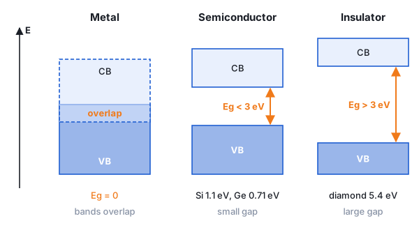
- Band picture: metals have overlapping or half-filled bands (); insulators have ; semiconductors have . Si , Ge , diamond .
- Intrinsic (pure) semiconductor: heat breaks covalent bonds and makes electron-hole pairs, so . At it is an insulator.
- A hole is a missing electron in a bond. It acts like a charge and moves opposite to electrons. Total current .
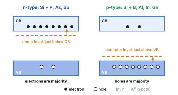
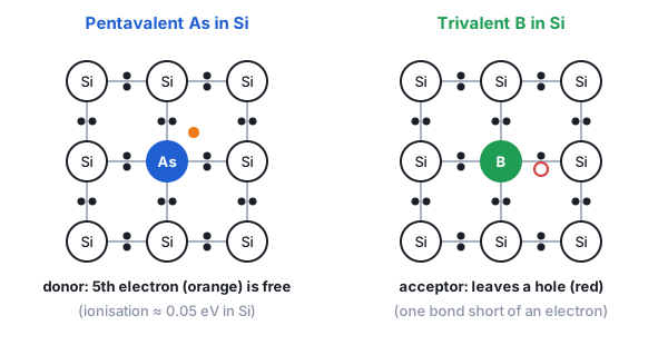
- n-type: dope with pentavalent P, As or Sb (donor). The fifth electron needs only about (Ge) or (Si) to become free. Electrons are majority carriers.
- p-type: dope with trivalent B, Al, In or Ga (acceptor). Each atom leaves a hole. Holes are majority carriers.
- Donor level lies just below the conduction band; acceptor level lies just above the valence band.
- Mass action law at equilibrium: . Doping raises the majority carriers and lowers the minority carriers below . Both n-type and p-type crystals stay electrically neutral.
- Resistance of a semiconductor falls as temperature rises (negative temperature coefficient), the opposite of a metal.
Formulas
- Intrinsic semiconductor
- Mass action law (thermal equilibrium, also for doped crystals)
- n-type with donor density
- Conductivity; = mobility,
- Photon needed to create an electron-hole pair
Tips, tricks and hacks
Common mistakes
✗ n-type is negatively charged because it has extra electrons.
✓ Each extra electron came with a donor ion of charge , so the crystal is neutral.
✗ Doping increases both electrons and holes.
✓ is fixed, so if majority carriers rise, minority carriers must fall.
✗ A hole is a positive particle like a positron.
✓ It is only a vacancy in a bond; its motion is really electrons moving the other way.
✗ At 0 K, a pure semiconductor conducts a little.
✓ At 0 K the valence band is full and the conduction band empty, so it is a perfect insulator.
NEET traps
NEET gives and and asks for holes: it is , much smaller than , not itself.
'Pure Si at room temperature is a good insulator' is false: it has a small but non-zero conductivity due to thermally generated pairs.
Option sets swap 'donor level below CB' and 'acceptor level above VB'; donors are near the CB, acceptors near the VB.
Quick check: Pure Si has . It is doped with boron atoms. The electron density is about
Answer: C. Boron makes it p-type with , so .
Topic 2 · 🔒
p-n junction and diode
Key points, graphs, every formula, tricks, common mistakes and NEET traps for this topic are inside Dhruv.
Start freeTopic 3 · 🔒
Rectifiers and special diodes
Key points, graphs, every formula, tricks, common mistakes and NEET traps for this topic are inside Dhruv.
Start freeTopic 4 · 🔒
Logic gates
Key points, graphs, every formula, tricks, common mistakes and NEET traps for this topic are inside Dhruv.
Start freePractise Semiconductor Electronics questions
Topic-wise practice from Level 1 to Level 3, NCERT-based questions and NEET PYQs, with a full solution after every answer.
Start practising free